If it is difficult to deal with obsolete equipment that is no longer being produced, PCB with no design data, etc., it is possible to modify and produce the board in the future by extracting key technical data such as circuit diagrams and gerbers from PCB samples that are being used and produced. We will support you as possible.
At least two boards are required for normal operation. One is used for circuit extraction and the other is used for comparison.
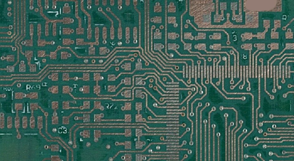
Layers Separation
Components are removed from the PCB for circuit extraction and separated by layers. After layer separtion using special equipment, and image of each layer is taken. Separated PCB become unusable, and are discarded after imaging.
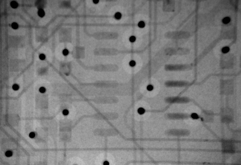
If there is only one PCB, the layer image is acquired by X-ray imaging without separating the PCB layer. In this case, time/cost is added by X-RAY operation, so it is advantageous in terms of cost to secure sufficient PCB.
Gerber file generation
Extract connection information from separated layer images. The connection diagram for each layer is automatically extracted using a dedicated S/W, and a gerber file is generated from this information. This gerber file makes it possible to produce the PCB.
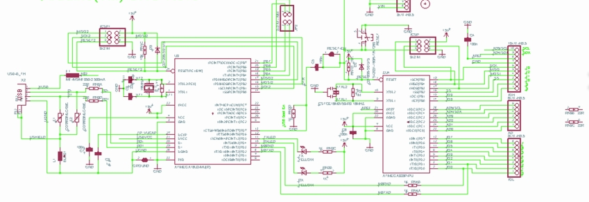
Schematic generation
Create a connection diagram from separate layer images. A special S/W is used to automatically extract the connection diagram for each layer, and use the inter-layer connection information to create the overall connection diagram. Adding the information of the electronic part removed from the PCB to this connection diagram completes the circuit diagram.
Currently, only Eagle CAD is supported.
Test
We create a sample PCB from the generated gerber/circuit diagram, and solder the relevant electronic components to it to check whether it works the same as the original PCB.